In power supplies (IP), PWM controllers, paired with a reference field-effect transistor, are widely used not only as part of TVs, but also in other electronic devices, including DVDs, receivers, and so on. They have the same principle of operation, the repair technique is also the same, only the schemes are different.
The proposed technique is to check and repair the PWM generator itself. I will take as a basis the IP of the HORIZONT 14A01 TV. Chassis SCCT-739M1, PWM controller UC3842AN.
The source can be roughly divided into three parts:
a) PWM generator
b) the power part of the primary circuits of the IP
c) secondary power circuits
So, PWM UC3842AN.
The scheme for supplying power to the microcircuit is standard, but there are some subtleties here.
At the moment of switching on, 300 volts, through R808, are fed to the 7th leg of the microcircuit. The microcircuit starts and gives a burst of pulses to the field-effect transistor. But the peculiarity of this microcircuit is that its starting voltage is higher, in our case by 2 volts, than the working one. And the R808 resistor is designed in such a way that on the 7th leg of the microcircuit, in the absence of recharge from the TPI (in our case, from the 3rd leg of the TPI through VD806), the voltage is working, but not starting! That is, if the IP did not start or went into defense, then there is no recharge from the VD806, and the microcircuit does not produce pulses.
So, if the power supply is unstable or does not start, or produces low voltages, the first step is to measure the voltage on the 7th leg, if it is lower than the working one (12-12.5 volts), then C816 should be replaced. If there is no voltage, then R808 is open, or the microcircuit is faulty.
Further. In case of other malfunctions, in particular when the field effect transistor fails or does not start.
To exclude the effect of the power part on the PWM itself, it is enough to unsolder the VT800 reference transistor and you can check and repair the generator with the voltage on, without fear for the failure of other elements of the IP and the rest of the circuit.
Based on the results of measuring the supply voltage and the output to the field-effect transistor, one can almost 100% judge the health of the microcircuit.
The device measures the voltage on the 7th leg. Everything is very clearly visible on the arrow device. The arrow from 12 volts should jump to 14. If so, then the power supply is in order. If not, then again the C816 or R808 is faulty, or the same microcircuit. As soon as the voltage on the 7th leg is normal, you should measure the voltage on the 6th leg, this is the output through R816 to the field effect transistor. If at the limit of 1-2-2.5 volts the arrow twitches, then the generator is working at 99% PWM. The field effect transistor is soldered back and, if necessary, the IP is repaired further.
Variants of this IC, produced by different manufacturers, may differ in prefixes, but necessarily contain the core 3842, 3843, 3844.
The microcircuit is available in SOIC-8 and SOIC-14 packages, but in the vast majority of cases, its modification is found in the DIP-8 package. On fig. 1 shows the pinout, and in fig. 2 - its block diagram and a typical IP diagram. The pin numbering is for the 8-pin package, the pin numbers in parentheses are for the SOIC-14 package. It should be noted that there are minor differences between the two versions of the IS. So, the version in the SOIC-14 package has separate power and ground pins for the output stage.
The uc3843 chip is designed to build stabilized pulsed power supplies with pulse-width modulation (PWM) on its basis. Since the power of the output stage of the IC is relatively small, and the amplitude of the output signal can reach the supply voltage of the microcircuit, an n-channel MOS transistor is used as a key in conjunction with this IC.
Rice. 1. UC3843 chip pinout
IC Pin Assignment for DIP Package.
1. Comp: This pin is connected to the output of the compensation error amplifier. For normal operation of the IC, it is necessary to compensate for the frequency response of the error amplifier; for this purpose, a capacitor with a capacity of about 100 pF is usually connected to this output, the second output of which is connected to output 2 of the IC.
2. Vfb: feedback input. the voltage at this pin is compared with the reference voltage generated inside the IC. The comparison result modulates the duty cycle of the output pulses, thus stabilizing the output voltage of the MT.
3.C/S: current limit signal. This output must be connected to a resistor in the source circuit of the key transistor (CT). With an increase in current through the CT (for example, in the event of an overload of the IP), the voltage across this resistor increases and, after reaching the threshold value, stops the IC and switches the CT to the closed state.
4.Rt/Ct: pin for connecting the timing RC circuit. The operating frequency of the internal oscillator is set by connecting a resistor R to the reference voltage Vref and a capacitor C (usually about 3000 pF) to ground. This frequency can be changed within a fairly wide range, from above it is limited by the speed of the CT, and from below by the power of the pulse transformer, which decreases with decreasing frequency. In practice, the frequency is selected in the range of 35 ... 85 kHz, but sometimes the IP works quite normally even at a much higher or much lower frequency. It should be noted that a capacitor with the greatest possible resistance to direct current should be used as a timing capacitor. In the author's practice, there were instances of ICs that generally refused to start when some types of ceramic capacitors were used as a timer.
5.Gnd: general conclusion. It should be noted that the common wire of the IP should in no case be connected to the common wire of the device in which it is used.
6. Out: output of the IC, connected to the gate of the CT through a resistor or a resistor and a diode connected in parallel (anode to the gate).
7. Vcc: IC power input. The considered IC has some very significant power-related features, which will be explained when considering a typical IC power circuit.
8. Vref: Internal reference voltage output, its output current is up to 50mA, voltage is 5V.
The exemplary voltage source is used to connect one of the arms of a resistive divider to it, designed to quickly adjust the output voltage of the IP, as well as to connect a timing resistor.
Let us now consider a typical circuit for switching on the IS, shown in Fig. 2.
Rice. 2. Typical wiring diagram UC3843
As can be seen from the circuit diagram, the IP is designed for a mains voltage of 115 V. The undoubted advantage of this type of IP is that it can be used with minimal modifications in a network with a voltage of 220 V, you just need:
* replace the diode bridge connected at the input of the IP with a similar one, but with a reverse voltage of 400 V;
* replace the electrolytic capacitor of the power filter, connected after the diode bridge, with an equal one in capacity, but with an operating voltage of 400 V;
* increase the value of the resistor R2 to 75 ... 80 kOhm;
* check the CT for the allowable drain-source voltage, which should be at least 600 V. As a rule, even in IP designed to operate on a 115 V network, CTs capable of operating on a 220 V network are used, but, of course, exceptions are possible. If the CT needs to be replaced, the author recommends the BUZ90.
As mentioned earlier, IP has some features related to its power supply. Let's consider them in more detail. At the first moment after turning on the IP in the network, the internal generator of the IC is not yet working, and in this mode it consumes very little current from the power circuits. To power the IC in this mode, the voltage obtained from the resistor R2 and accumulated on the capacitor C2 is sufficient. When the voltage on these capacitors reaches a value of 16 ... 18 V, the IC generator starts, and it begins to generate CT control pulses at the output. Voltage appears on the secondary windings of the transformer T1, including windings 3-4. This voltage is rectified by pulse diode D3, filtered by capacitor C3, and fed through diode D2 to the power supply circuit of the IC. As a rule, a zener diode D1 is included in the power circuit, limiting the voltage at the level of 18 ... 22 V. After the IC has entered the operating mode, it begins to track changes in its supply voltage, which is fed through the divider R3, R4 to the feedback input Vfb. By stabilizing its own supply voltage, the IC actually stabilizes all other voltages taken from the secondary windings of the pulse transformer.
In case of short circuits in the circuits of the secondary windings, for example, as a result of a breakdown of electrolytic capacitors or diodes, the energy losses in the pulse transformer increase sharply. As a result, the voltage received from windings 3-4 is not enough to maintain the normal operation of the IC. The internal oscillator turns off, a low-level voltage appears at the output of the IC, turning the CT into a closed state, and the microcircuit is again in low power mode. After a while, its supply voltage rises to a level sufficient to start the internal generator, and the process repeats. In this case, characteristic clicks (clicks) are heard from the transformer, the repetition period of which is determined by the values of the capacitor C2 and resistor R2.
When repairing a power supply, situations sometimes arise when a characteristic ticking is heard from the transformer, but a thorough check of the secondary circuits shows that there is no short circuit in them. In this case, you need to check the power circuits of the IC itself. For example, in the author's practice, there were cases when the capacitor C3 was broken. A common reason for this behavior of the power supply is a break in the rectifier diode D3 or the decoupling diode D2.
When a powerful CT breaks down, as a rule, it has to be changed together with the IC. The fact is that the gate of the CT is connected to the output of the IC through a resistor of a very small value, and in the event of a breakdown of the CT, a high voltage from the primary winding of the transformer enters the output of the IC. The author categorically recommends that in case of a malfunction of the CT, it should be changed along with the IC, fortunately, its cost is low. Otherwise, there is a risk of “killing” a new CT, because if a high voltage level from a broken IC output is present on its gate for a long time, then it will fail due to overheating.
Some other features of this IP were noticed. In particular, during a breakdown of the CT, the resistor R10 in the source circuit very often burns out. When replacing this resistor, you should adhere to the nominal value of 0.33 ... 0.5 Ohm. It is especially dangerous to overvalue the resistor. In this case, as practice has shown, at the first inclusion of the IP in the network, both the microcircuit and the transistor fail.
In some cases, the failure of the IP occurs due to the breakdown of the zener diode D1 in the power supply circuit of the IC. In this case, the IC and CT, as a rule, remain serviceable, it is only necessary to replace the zener diode. In the event of a break in the zener diode, both the IC itself and the CT often fail. For replacement, the author recommends using domestic KS522 zener diodes in a metal case. Having bitten or soldered a faulty standard zener diode, you can solder the KS522 with the anode to terminal 5 of the IC, the cathode to terminal 7 of the IC. As a rule, after such a replacement, similar malfunctions no longer occur.
You should pay attention to the health of the potentiometer used to adjust the output voltage of the IP, if any in the circuit. It is not in the above circuit, but it is not difficult to introduce it by including resistors R3 and R4 in the gap. Pin 2 of the IC must be connected to the slider of this potentiometer. I note that in some cases such refinement is simply necessary. Sometimes, after replacing the IC, the output voltages of the SP are too high or too low, and there is no adjustment. In this case, you can either turn on the potentiometer, as mentioned above, or choose the value of the resistor R3.
According to the author's observation, if high-quality components are used in the IP, and it is not operated in extreme conditions, its reliability is quite high. In some cases, the reliability of the IP can be improved by using a resistor R1 with a slightly larger rating, for example, 10 ... 15 ohms. In this case, power-on transients are much more relaxed. In video monitors and TVs, this must be done without affecting the kinescope demagnetization circuit, i.e., the resistor should in no case be included in the break in the common power circuit, but only in the connection circuit of the IP itself.
You can download datasheet on uc3843
PWM UC3842AN
The UC3842 is a PWM controller circuit with current and voltage feedback for controlling the key stage on an n-channel MOS transistor, discharging its input capacitance with a forced current of up to 0.7A. The SMPS controller chip consists of the UC384X (UC3843, UC3844, UC3845) series of PWM controller chips. The UC3842 core is specially designed for long-term operation with a minimum number of external discrete components. The UC3842 PWM controller features precise duty cycle control, temperature compensation and low cost. A feature of the UC3842 is the ability to operate within a 100% duty cycle (for example, the UC3844 operates with a duty cycle of up to 50%.). The domestic analogue of UC3842 is 1114EU7. Power supplies made on the UC3842 chip are distinguished by increased reliability and ease of execution.
Rice. Type table.
This table gives a complete picture of the differences between the UC3842, UC3843, UC3844, UC3845 microcircuits.
General description.
For those who want to get more deeply acquainted with the UC384X series PWM controllers, the following material is recommended.
- Datasheet UC3842B (download)
- Datasheet 1114EU7 domestic analogue of the UC3842A chip (download).
- Article "Flyback converter", Dmitry Makashev (download).
- Description of the operation of PWM controllers of the UCX84X series (download).
- Article "Evolution of flyback switching power supplies", S. Kosenko (download). The article was published in the magazine "Radio" No. 7-9 for 2002.
The document from STC SIT, the most successful description in Russian for PWM UC3845 (K1033EU16), is highly recommended for review. (Download).
The difference between the UC3842A and UC3842B chips, A consumes less current until the start.
UC3842 has two versions of the package 8pin and 14pin, the pinout of these versions is significantly different. Further, only the variant of the 8pin package will be considered.
A simplified block diagram is necessary to understand the principle of operation of a PWM controller.
Rice. Block diagram of UC3842
A structural diagram in a more detailed version is necessary for diagnosing and testing the performance of the microcircuit. Since we are considering the 8pin version, Vc is 7pin, PGND is 5pin.
Rice. UC3842 block diagram (detailed version)
Rice. Pinout UC3842
There should be material on the purpose of the conclusions, but it is much more convenient to read and look at the practical circuit for switching on the UC3842 PWM controller. The circuit is drawn so well that it makes it much easier to understand the purpose of the pins of the microcircuit.
Rice. Wiring diagram UC3842 on the example of a power supply for TV
1. Comp:(rus. Correction) error amplifier output. For normal operation of the PWM controller, it is necessary to compensate for the frequency response of the error amplifier; for this purpose, a capacitor with a capacity of about 100 pF is usually connected to the indicated output, the second output of which is connected to output 2 of the IC. If the voltage at this pin is lowered below 1 volt, then the pulse duration will decrease at output 6 of the microcircuit, thereby reducing the power of this PWM controller.
2. Vfb: (rus. Feedback voltage) feedback input. The voltage at this pin is compared with the reference voltage generated inside the UC3842 PWM controller. The result of the comparison modulates the duty cycle of the output pulses, as a result, the output voltage of the power supply stabilizes. Formally, the second output serves to reduce the duration of the output pulses, if you apply more than +2.5 volts to it, then the pulses will be reduced and the microcircuit will reduce the output power.
3.C/S: (second designation I feel) (rus. Current feedback) current limit signal. This pin must be connected to a resistor in the source circuit of the switching transistor. At the moment of overloading the MOS transistor, the voltage across the resistance increases and, when a certain threshold is reached, the UC3842A stops its operation, closing the output transistor. Simply put, the output serves to turn off the pulse at the output when a voltage above 1 volt is applied to it.
4.Rt/Ct: (rus. Frequency reference) connection of the timing RC circuit required to set the frequency of the internal generator. R is connected to Vref - the reference voltage, and C to the common wire (usually several tens of nF are selected). This frequency can be changed within a fairly wide range, from above it is limited by the speed of the key transistor, and from below by the power of the pulse transformer, which decreases with decreasing frequency. In practice, the frequency is selected in the range of 35 ... 85 kHz, but sometimes the power supply works quite normally even at a much higher or much lower frequency.
For a timing RC circuit, it is better to abandon ceramic capacitors.
5.Gnd: (rus. General) general conclusion. The common terminal must not be connected to the body of the circuit. This "hot" ground is connected to the body of the device through a pair of capacitors.
6. Out: (rus. Exit) the output of the PWM controller is connected to the gate of the key transistor through a resistor or a resistor and a diode connected in parallel (with the anode to the gate).
7. Vcc: (rus. Nutrition) power input of the PWM controller, this output of the microcircuit is supplied with a supply voltage in the range from 16 volts to 34 volts, please note that this microcircuit has a built-in Schmidt trigger (UVLO), which turns on the microcircuit if the supply voltage exceeds 16 volts, if the voltage for some reason it will become lower than 10 volts (for other microcircuits of the UC384X series, the ON / OFF values may differ, see the Table of Ratings), it will be disconnected from the supply voltage. The microcircuit also has overvoltage protection: if the supply voltage on it exceeds 34 volts, the microcircuit will turn off.
8. Vref: output of an internal reference voltage source, its output current is up to 50 mA, voltage is 5 V. It is connected to one of the divider arms and is used to quickly adjust the U output of the entire power supply.
A bit of theory.
Shutdown circuit when the input voltage drops.
Rice. Shutdown circuit when the input voltage drops.
The Under-Voltage LockOut or UVLO circuit ensures that Vcc is equal to the voltage that makes the UC384x fully operational to turn on the output stage. On Fig. it is shown that the UVLO circuit has on and off threshold voltages, the values of which are 16 and 10, respectively. A hysteresis of 6V prevents erratic switching on and off during power-up.
Generator.
Rice. Generator UC3842.
The frequency-setting capacitor Ct is charged from Vref(5V) through the frequency-setting resistor Rt, and is discharged by the internal current source.
The UC3844 and UC3845 have a built-in counting flip-flop that is used to obtain a maximum oscillator duty cycle of 50%. Therefore, the generators of these microcircuits must be set to a switching frequency twice as high as desired. The UC3842 and UC3843 chip generators are set to the desired switching frequency. The maximum operating frequency of the UC3842/3/4/5 family generators can reach 500 kHz.
Reading and current limiting.
Rice. Organization of current feedback.
The current-to-voltage conversion is performed with an external resistor Rs connected to ground. RC filter to suppress output key spikes. The inverting input of the current sense comparator UC3842 is internally biased by 1V. Current limiting occurs if the voltage at pin 3 reaches this threshold.
Error signal amplifier.
Rice. Structural diagram of the error signal amplifier.
The non-inverting error input has no separate pin and is internally biased by 2.5 volts. The output of the error amplifier is connected to pin 1 to connect an external compensating circuit, allowing the user to control the frequency response of the converter's closed loop feedback.
Rice. Scheme of the compensating circuit.
A compensating circuit suitable for stabilizing any converter circuit with additional current feedback, except flyback and boost converters operating with inductor current.
Blocking methods.
There are two ways to block the UC3842 chip:
increasing the voltage at pin 3 above the level of 1 volt,
or pulling up the voltage at pin 1 to a level not exceeding the voltage drop across two diodes, relative to the ground potential.
Each of these methods results in a logic HIGH voltage level at the output of the PWM coparator (structural diagram). Since the main (default) state of the PWM latch is reset, the output of the PWM comparator will be held LOW until the state on pins 1 and/or 3 changes in the next clock period (the period following the one in question). clock period when a situation has arisen that requires blocking the microcircuit).
Connection diagram.
The simplest connection scheme for the UC3842 PWM controller is purely academic. The circuit is the simplest generator. Despite its simplicity, this scheme works.
Rice. The simplest switching scheme 384x
As can be seen from the diagram, the UC3842 PWM controller requires only an RC circuit and power to operate.
Scheme of switching on the PWM controller of the UC3842A PWM controller, using the example of a TV power supply.
Rice. Power supply diagram for UC3842A.
The diagram gives a visual and simple representation of the use of the UC3842A in a simple power supply. Scheme for easier reading, slightly modified. The full version of the circuit can be found in the PDF document "Power supplies 106 circuits" Tovarnitsky N.I.
Scheme of switching on the PWM controller of the UC3843 PWM controller, using the example of the power supply of the D-Link router, JTA0302E-E.
Rice. Schematic diagram of the power supply on the UC3843.
Although the circuit is made according to the standard inclusion for UC384X, however, R4 (300k) and R5 (150) are deduced from the standards. However, successfully, and most importantly, logically selected circuits help to understand the principle of operation of the power supply.
Power supply on a UC3842 PWM controller. The scheme is not intended to be repeated, but is for informational purposes only.
Rice. The standard inclusion scheme from datasheet-a (the scheme has been slightly modified for easier understanding).
Repair of the Power Supply based on PWM UC384X.
Checking with an external power supply.
Rice. Simulation of the PWM controller.
Checking the operation is carried out without soldering the microcircuit from the power supply. The power supply must be disconnected from the 220V network before carrying out diagnostics!
From an external stabilized power supply, apply voltage to pin 7 (Vcc) of the microcircuit, a voltage greater than the UVLO turn-on voltage, in the general case, more than 17V. In this case, the UC384X PWM controller should work. If the supply voltage is less than the UVLO turn-on voltage (16V / 8.4V), then the microcircuit will not start. You can read more about UVLO here.
Checking the internal voltage reference.
ExaminationUVLO
If the external power supply allows voltage regulation, then it is advisable to check the operation of the UVLO. By changing the voltage on pin 7(Vcc) of the pin within the UVLO voltage range, the reference voltage on pin 8(Vref) = +5V should not change.
It is not recommended to apply voltage of 34V and higher to pin 7(Vcc). It is possible that there is a protective zener diode in the power supply circuit of the UC384X PWM controller, then it is not recommended to apply this zener diode above the operating voltage.
Checking the operation of the generator and external circuits of the generator.
You will need an oscilloscope to check. Pin 4(Rt/Ct) should have a stable "saw".
Checking the output control signal.
You will need an oscilloscope to check. Ideally, pin 6(Out) should have square wave pulses. However, the circuit under study may differ from the one shown, and then it will be necessary to turn off the external feedback circuits. The general principle is shown in fig. - with this inclusion, the UC384X PWM controller is guaranteed to start.
Rice. UC384x operation with feedback circuits disabled.
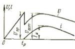
Rice. An example of real signals when simulating the operation of a PWM controller.
If the power supply unit with a UC384x PWM controller does not turn on or turns on with a long delay, then check by replacing the electrolytic capacitor that filters the power supply (pin 7) of this m / s. It is also necessary to check the elements of the initial start circuit (usually two 33-100kOhm resistors connected in series).
When replacing a power (field) transistor in a power supply unit with a control m / s 384x, it is imperative to check the resistor that acts as a current sensor (it is at the source of the field). A change in its resistance at a nominal value in fractions of an ohm is very difficult to detect with an ordinary tester! An increase in the resistance of this resistor leads to a false operation of the PSU current protection. At the same time, it is possible to look for the reasons for PSU overload in secondary circuits for a very long time, although they are not there at all.
Chip UC3842(UC3843)- is a PWM controller circuit with current and voltage feedback for controlling a key stage on an n-channel MOS transistor, providing a discharge of its input capacitance with a forced current of up to 0.7A. Chip SMPS the controller consists of a series of chips UC384X (UC3843, UC3844, UC3845) PWM controllers. Core UC3842 specially designed for long-term operation with a minimum number of external discrete components. PWM controller UC3842 features precise duty cycle control, temperature compensation and low cost. feature UC3842 is the ability to work within 100% of the duty cycle (for example UC3844 works with fill factor up to 50%.). Domestic analogue UC3842 is 1114EU7. Power supplies made on a microcircuit UC3842 characterized by increased reliability and ease of execution.
Differences in supply voltage UC3842 and UC3843:
UC3842_________| 16 Volt / 10 Volt
UC3843_________| 8.4 Volt / 7.6 Volt
Differences in the duty cycle of the pulses:
UC3842, UC3843__| 0% / 98%
Tsokolevka UC3842(UC3843) shown in fig. 1
The simplest switching circuit is shown in fig. 2 
The UC3842 PWM controller chip is the most common when building monitor power supplies. In addition, these microcircuits are used to build switching voltage regulators in horizontal scanners of monitors, which are both high voltage stabilizers and raster correction circuits. The UC3842 chip is often used to control the key transistor in system power supplies (single-cycle) and in printer power supplies. In a word, this article will be of interest to absolutely all specialists, one way or another connected with power sources.
The failure of the UC 3842 chip in practice occurs quite often. Moreover, as the statistics of such failures show, the breakdown of a powerful field-effect transistor, which is controlled by this microcircuit, becomes the cause of the microcircuit malfunction. Therefore, when replacing the power transistor of the power supply in the event of a malfunction, it is strongly recommended to check the UC 3842 control chip.
There are several methods for testing and diagnosing a microcircuit, but the most effective and easiest to put into practice in a poorly equipped workshop are checking the output resistance and simulating the operation of a microcircuit using an external power source.
For this work you will need the following devices:
There are two main ways to check the health of the microcircuit:
The functional diagram is shown in Fig. 1, and the location and purpose of the contacts in Fig. 2.
Checking the output resistance of the microcircuit
Very accurate information about the health of the microcircuit is given by its output impedance, since during breakdowns of the power transistor, a high-voltage voltage pulse is applied precisely to the output stage of the microcircuit, which ultimately causes its failure.
The output impedance of the microcircuit must be infinitely large, since its output stage is a quasi-complementary amplifier.
You can check the output resistance with an ohmmeter between pins 5 (GND) and 6 (OUT) of the microcircuit (Fig. 3), and the polarity of connecting the measuring device does not matter. Such a measurement is best done with a soldered microcircuit. In the event of a breakdown of the microcircuit, this resistance becomes equal to several ohms.
If you measure the output resistance without soldering the microcircuit, then you must first unsolder the faulty transistor, since in this case its broken gate-source junction may "ring". In addition, it should be taken into account that usually the circuit has a terminating resistor connected between the output of the microcircuit and the "case". Therefore, a serviceable microcircuit may have an output impedance during testing. Although, it usually does not happen less than 1 kOhm.
Thus, if the output resistance of the microcircuit is very small or has a value close to zero, then it can be considered faulty.
Modeling the operation of the microcircuit
Such a check is carried out without soldering the microcircuit from the power supply. The power supply must be turned off before carrying out diagnostics!
The essence of the test is to supply power to the microcircuit from an external source and analyze its characteristic signals (amplitude and shape) using an oscilloscope and a voltmeter.
The workflow includes the following steps:
- 1) Unplug the monitor from the AC power (disconnect the power cable).
- 2) From an external stabilized current source, apply a supply voltage of more than 16V to pin 7 of the microcircuit (for example, 17-18 V). In this case, the microcircuit should start. If the supply voltage is less than 16 V, then the microcircuit will not start.
- 3) Using a voltmeter (or oscilloscope), measure the voltage at pin 8 (VREF) of the microcircuit. There should be a reference stabilized voltage of +5 V DC.
- 4) By changing the output voltage of the external current source, make sure that the voltage on pin 8 is stable. (The voltage of the current source can be changed from 11 V to 30 V, with a further decrease or increase in voltage, the microcircuit will turn off, and the voltage on pin 8 will disappear).
- 5) Use an oscilloscope to check the signal on pin 4 (CR). In the case of a working microcircuit and its external circuits, there will be a linearly changing voltage (sawtooth) on this contact.
- 6) By changing the output voltage of the external current source, make sure that the amplitude and frequency of the sawtooth voltage on pin 4 are stable.
- 7) Using an oscilloscope, check for the presence of rectangular pulses on pin 6 (OUT) of the microcircuit (output control pulses).
If all of these signals are present and behave in accordance with the above rules, then we can conclude that the microcircuit is in good condition and that it is functioning correctly.
In conclusion, I would like to note that in practice it is worth checking the serviceability of not only the microcircuit, but also the elements of its output circuits (Fig. 3). First of all, these are resistors R1 and R2, diode D1, zener diode ZD1, resistors R3 and R4, which form a current protection signal. These elements often turn out to be faulty during breakdowns.
Switching power supplies based on the UC3842 chip
The article is devoted to the device, repair and refinement of power supplies for a wide range of equipment, made on the basis of the UC3842 chip. Some of the information provided was obtained by the author as a result of personal experience and will help you not only avoid mistakes and save time during repairs, but also increase the reliability of the power supply. Since the second half of the 90s, a huge number of TVs, video monitors, faxes and other devices have been produced, in the power supplies (IP) of which the UC3842 integrated circuit (hereinafter referred to as the IC) is used. Apparently, this is due to its low cost, a small number of discrete elements needed for its "body kit" and, finally, fairly stable characteristics of the integrated circuit, which is also important. Variants of this IC, produced by different manufacturers, may differ in prefixes, but necessarily contain the 3842 core.
The UC3842 is available in SOIC-8 and SOIC-14 packages, but in the vast majority of cases, its modification is found in a DIP-8 package. On fig. 1 shows the pinout, and in fig. 2 - its block diagram and a typical IP diagram. The pin numbering is for the 8-pin package, the pin numbers in parentheses are for the SOIC-14 package. It should be noted that there are minor differences between the two versions of the IS. So, the version in the SOIC-14 package has separate power and ground pins for the output stage.
The UC3842 chip is designed to build stabilized pulsed power supplies with pulse-width modulation (PWM) on its basis. Since the power of the output stage of the IC is relatively small, and the amplitude of the output signal can reach the supply voltage of the microcircuit, an n-channel MOS transistor is used as a key in conjunction with this IC.
Rice. 1. UC3842 pinout (top view)
Let's take a closer look at the assignment of IC pins for the most common eight-pin package.
- Comp: This pin is connected to the output of the compensation error amplifier. For normal operation of the IC, it is necessary to compensate for the frequency response of the error amplifier; for this purpose, a capacitor with a capacity of about 100 pF is usually connected to this output, the second output of which is connected to output 2 of the IC.
- vfb: feedback input. The voltage at this pin is compared with the reference voltage generated inside the IC. The comparison result modulates the duty cycle of the output pulses, thus stabilizing the output voltage of the MT.
- C/S: current limit signal. This output must be connected to a resistor in the source circuit of the key transistor (CT). With an increase in current through the CT (for example, in the event of an overload of the IP), the voltage across this resistor increases and, after reaching the threshold value, stops the IC and switches the CT to the closed state.
- Rt/Ct: pin for connecting the timing RC circuit. The operating frequency of the internal oscillator is set by connecting a resistor R to the reference voltage Vref and a capacitor C (usually about 3000 pF) to ground. This frequency can be changed within a fairly wide range, from above it is limited by the speed of the CT, and from below by the power of the pulse transformer, which decreases with decreasing frequency. In practice, the frequency is selected in the range of 35 ... 85 kHz, but sometimes the IP works quite normally even at a much higher or much lower frequency. It should be noted that a capacitor with the greatest possible resistance to direct current should be used as a timing capacitor. In the author's practice, there were instances of ICs that generally refused to start when some types of ceramic capacitors were used as a timer.
- Gnd: general conclusion. It should be noted that the common wire of the IP should in no case be connected to the common wire of the device in which it is used.
- out: output of the IC, connected to the gate of the CT through a resistor or a resistor and a diode connected in parallel (anode to the gate).
- Vcc: IC power input. The considered IC has some very significant power-related features, which will be explained when considering a typical IC power circuit.
- Vref: Internal reference voltage output, its output current is up to 50mA, voltage is 5V.
The exemplary voltage source is used to connect one of the arms of a resistive divider to it, designed to quickly adjust the output voltage of the IP, as well as to connect a timing resistor.
Let us now consider a typical circuit for switching on the IS, shown in Fig. 2.
Rice. 2. Typical wiring diagram UC3862
As can be seen from the circuit diagram, the IP is designed for a mains voltage of 115 V. The undoubted advantage of this type of IP is that it can be used with minimal modifications in a network with a voltage of 220 V, you just need:
- replace the diode bridge connected at the input of the IP with a similar one, but with a reverse voltage of 400 V;
- replace the electrolytic capacitor of the power filter, connected after the diode bridge, with an equal one in capacity, but with an operating voltage of 400 V;
- increase the value of the resistor R2 to 75 ... 80 kOhm;
- check the CT for the allowable drain-source voltage, which should be at least 600 V. As a rule, even in IPs designed to operate on a 115 V network, CTs capable of operating on a 220 V network are used, but, of course, exceptions are possible. If the CT needs to be replaced, the author recommends the BUZ90.
As mentioned earlier, IP has some features related to its power supply. Let's consider them in more detail. At the first moment after turning on the IP in the network, the internal generator of the IC is not yet working, and in this mode it consumes very little current from the power circuits. To power the IC in this mode, the voltage obtained from the resistor R2 and accumulated on the capacitor C2 is sufficient. When the voltage on these capacitors reaches a value of 16 ... 18 V, the IC generator starts, and it begins to generate CT control pulses at the output. Voltage appears on the secondary windings of the transformer T1, including windings 3-4. This voltage is rectified by pulse diode D3, filtered by capacitor C3, and fed through diode D2 to the power supply circuit of the IC. As a rule, a zener diode D1 is included in the power circuit, limiting the voltage at the level of 18 ... 22 V. After the IC has entered the operating mode, it begins to track changes in its supply voltage, which is fed through the divider R3, R4 to the feedback input Vfb. By stabilizing its own supply voltage, the IC actually stabilizes all other voltages taken from the secondary windings of the pulse transformer.
In case of short circuits in the circuits of the secondary windings, for example, as a result of a breakdown of electrolytic capacitors or diodes, the energy losses in the pulse transformer increase sharply. As a result, the voltage received from windings 3-4 is not enough to maintain the normal operation of the IC. The internal oscillator turns off, a low-level voltage appears at the output of the IC, turning the CT into a closed state, and the microcircuit is again in low power mode. After a while, its supply voltage rises to a level sufficient to start the internal generator, and the process repeats. In this case, characteristic clicks (clicks) are heard from the transformer, the repetition period of which is determined by the values of the capacitor C2 and resistor R2.
When repairing a power supply, situations sometimes arise when a characteristic ticking is heard from the transformer, but a thorough check of the secondary circuits shows that there is no short circuit in them. In this case, you need to check the power circuits of the IC itself. For example, in the author's practice, there were cases when the capacitor C3 was broken. A common reason for this behavior of the power supply is a break in the rectifier diode D3 or the decoupling diode D2.
When a powerful CT breaks down, as a rule, it has to be changed together with the IC. The fact is that the gate of the CT is connected to the output of the IC through a resistor of a very small value, and in the event of a breakdown of the CT, a high voltage from the primary winding of the transformer enters the output of the IC. The author categorically recommends that in case of a malfunction of the CT, it should be changed along with the IC, fortunately, its cost is low. Otherwise, there is a risk of “killing” a new CT, because if a high voltage level from a broken IC output is present on its gate for a long time, then it will fail due to overheating.
Some other features of this IP were noticed. In particular, during a breakdown of the CT, the resistor R10 in the source circuit very often burns out. When replacing this resistor, you should adhere to the nominal value of 0.33 ... 0.5 Ohm. It is especially dangerous to overvalue the resistor. In this case, as practice has shown, at the first inclusion of the IP in the network, both the microcircuit and the transistor fail.
In some cases, the failure of the IP occurs due to the breakdown of the zener diode D1 in the power supply circuit of the IC. In this case, the IC and CT, as a rule, remain serviceable, it is only necessary to replace the zener diode. In the event of a break in the zener diode, both the IC itself and the CT often fail. For replacement, the author recommends using domestic KS522 zener diodes in a metal case. Having bitten or soldered a faulty standard zener diode, you can solder the KS522 with the anode to terminal 5 of the IC, the cathode to terminal 7 of the IC. As a rule, after such a replacement, similar malfunctions no longer occur.
You should pay attention to the health of the potentiometer used to adjust the output voltage of the IP, if any in the circuit. It is not in the above circuit, but it is not difficult to introduce it by including resistors R3 and R4 in the gap. Pin 2 of the IC must be connected to the slider of this potentiometer. I note that in some cases such refinement is simply necessary. Sometimes, after replacing the IC, the output voltages of the SP are too high or too low, and there is no adjustment. In this case, you can either turn on the potentiometer, as mentioned above, or choose the value of the resistor R3.
According to the author's observation, if high-quality components are used in the IP, and it is not operated in extreme conditions, its reliability is quite high. In some cases, the reliability of the IP can be improved by using a resistor R1 with a slightly larger rating, for example, 10 ... 15 ohms. In this case, power-on transients are much more relaxed. In video monitors and TVs, this must be done without affecting the kinescope demagnetization circuit, i.e., the resistor should in no case be included in the break in the common power circuit, but only in the connection circuit of the IP itself.
Alexey Kalinin
"Repair of electronic equipment"