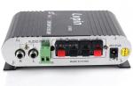
Charger for UC3842/UC3843 with voltage and current regulation
The charger described here is designed to charge lead-acid batteries. There are two adjustments: voltage and current. When one of these adjustments is triggered, the corresponding LED lights up, which is very convenient. The circuit and printed circuit board were taken from the radiocat forum:
The device is assembled on the common UC3842/UC3843 microcircuit. We have already described its use in power supplies. In this circuit, adjustment occurs at 1 pin. The power part is standard, the microcircuit is powered from a separate winding on the return stroke.

click to enlarge
Voltage and current adjustments were made according to a diagram from forum member FolksDoich. The TL431 contains a reference voltage source. Voltage and current adjustments are made on the halves of the LM358 op-amp. If you use LEDs as VD6 and VD7, they will indicate the current adjustment by their glow, which can be useful. For example, if the VD7 LED is lit, then current limitation occurs. The same with VD6, but in terms of voltage.
This circuit is designed to charge the battery with a current of up to 6 amperes, so it is proposed to parallel four electrolytic capacitors at the output, because one at high current will not work for long. Of course they all have to be LOW ESR.
How can this scheme be improved? If you use it to assemble not a charger, but a power supply, adjustable within certain limits, then you can make the usual improvements described in the previous article. In particular, you can power the UC3842/UC3843 microcircuit in direct mode, and use a separate transformer winding to power the op-amp and PC817. All this is justified only if it is necessary to expand the voltage regulation range.
In addition to LEDs, the circuit can be supplemented with an ammeter and voltmeter, both pointer and digital devices that show the value of voltage and current, and, possibly, also calculate the load power and control the cooling fan.
If you choose the right power field-effect transistor, its heating should be insignificant. It should be mentioned that in the diagram they forgot to draw a 2.2 nF capacitor between the hot and cold parts.

PCB: charger_12v_6a.lay6

There is another variation of this scheme in this form:

click to enlarge
Printed circuit boards from FolksDoich for devices of different power, the second board - up to 10 amperes. The UC384x chip is located on a separate small board, mounted vertically on the main one.

Who has not encountered in their practice the need to charge a battery and, disappointed in the lack of a charger with the necessary parameters, was forced to purchase a new charger in a store, or reassemble the necessary circuit?
So I have repeatedly had to solve the problem of charging various batteries when there was no suitable charger at hand. I had to quickly assemble something simple, in relation to a specific battery.
The situation was tolerable until the need for mass preparation and, accordingly, charging the batteries arose. It was necessary to produce several universal chargers - inexpensive, operating in a wide range of input and output voltages and charging currents.
The charger circuits proposed below were developed for charging lithium-ion batteries, but it is possible to charge other types of batteries and composite batteries (using the same type of cells, hereinafter referred to as AB).
All presented schemes have the following main parameters:
input voltage 15-24 V;
charge current (adjustable) up to 4 A;
output voltage (adjustable) 0.7 - 18 V (at Uin=19V).
All circuits were designed to work with power supplies from laptops or to work with other power supplies with DC output voltages from 15 to 24 Volts and were built on widespread components that are present on the boards of old computer power supplies, power supplies of other devices, laptops, etc.
Memory circuit No. 1 (TL494)

The memory in Scheme 1 is a powerful pulse generator operating in the range from tens to a couple of thousand hertz (the frequency varied during research), with an adjustable pulse width.
The battery is charged by current pulses limited by feedback formed by the current sensor R10, connected between the common wire of the circuit and the source of the switch on the field-effect transistor VT2 (IRF3205), filter R9C2, pin 1, which is the “direct” input of one of the error amplifiers of the TL494 chip.
The inverse input (pin 2) of the same error amplifier is supplied with a comparison voltage, regulated by a variable resistor PR1, from a reference voltage source built into the chip (ION - pin 14), which changes the potential difference between the inputs of the error amplifier.
As soon as the voltage value on R10 exceeds the voltage value (set by the variable resistor PR1) at pin 2 of the TL494 microcircuit, the charging current pulse will be interrupted and resumed again only at the next cycle of the pulse sequence generated by the microcircuit generator.
By thus adjusting the width of the pulses on the gate of transistor VT2, we control the battery charging current.
Transistor VT1, connected in parallel with the gate of a powerful switch, provides the necessary discharge rate of the gate capacitance of the latter, preventing “smooth” locking of VT2. In this case, the amplitude of the output voltage in the absence of a battery (or other load) is almost equal to the input supply voltage.
With an active load, the output voltage will be determined by the current through the load (its resistance), which allows this circuit to be used as a current driver.
When charging the battery, the voltage at the switch output (and, therefore, at the battery itself) will tend to increase over time to a value determined by the input voltage (theoretically) and this, of course, cannot be allowed, knowing that the voltage value of the lithium battery being charged should be limited to 4.1V (4.2V). Therefore, the memory uses a threshold device circuit, which is a Schmitt trigger (hereinafter - TS) on an op-amp KR140UD608 (IC1) or on any other op-amp.
When the required voltage value on the battery is reached, at which the potentials at the direct and inverse inputs (pins 3, 2 - respectively) of IC1 are equal, a high logical level (almost equal to the input voltage) will appear at the output of the op-amp, causing the LED indicating the end of charging HL2 and the LED to light up optocoupler VH1 which will open its own transistor, blocking the supply of pulses to output U1. The key on VT2 will close and the battery will stop charging.
Once the battery is charged, it will begin to discharge through the reverse diode built into VT2, which will be directly connected in relation to the battery and the discharge current will be approximately 15-25 mA, taking into account the discharge also through the elements of the TS circuit. If this circumstance seems critical to someone, a powerful diode (preferably with a low forward voltage drop) should be placed in the gap between the drain and the negative terminal of the battery.
The TS hysteresis in this version of the charger is chosen such that the charge will begin again when the voltage on the battery drops to 3.9 V.
This charger can also be used to charge series-connected lithium (and other) batteries. It is enough to calibrate the required response threshold using variable resistor PR3.
So, for example, a charger assembled according to scheme 1 operates with a three-section serial battery from a laptop, consisting of dual elements, which was mounted to replace the nickel-cadmium battery of a screwdriver.
The power supply from the laptop (19V/4.7A) is connected to the charger, assembled in the standard case of the screwdriver charger instead of the original circuit. The charging current of the “new” battery is 2 A. At the same time, transistor VT2, working without a radiator, heats up to a maximum temperature of 40-42 C.
The charger is switched off, naturally, when the battery voltage reaches 12.3V.
The TS hysteresis when the response threshold changes remains the same as a PERCENTAGE. That is, if at a shutdown voltage of 4.1 V, the charger was turned on again when the voltage dropped to 3.9 V, then in this case the charger was turned on again when the voltage on the battery decreased to 11.7 V. But if necessary, the hysteresis depth can change.
Charger Threshold and Hysteresis Calibration
Calibration occurs using an external voltage regulator (laboratory power supply).The upper threshold for triggering the TS is set.
1. Disconnect the upper pin PR3 from the charger circuit.
2. We connect the “minus” of the laboratory power supply (hereinafter referred to as the LBP everywhere) to the negative terminal for the battery (the battery itself should not be in the circuit during setup), the “plus” of the LBP to the positive terminal for the battery.
3. Turn on the charger and LBP and set the required voltage (12.3 V, for example).
4. If the end of charge indication is on, rotate the PR3 slider down (according to the diagram) until the indication goes out (HL2).
5. Slowly rotate the PR3 engine upward (according to the diagram) until the indication lights up.
6. Slowly reduce the voltage level at the output of the LBP and monitor the value at which the indication goes out again.
7. Check the level of operation of the upper threshold again. Fine. You can adjust the hysteresis if you are not satisfied with the voltage level that turns on the charger.
8. If the hysteresis is too deep (the charger is switched on at a too low voltage level - below, for example, the battery discharge level), turn the PR4 slider to the left (according to the diagram) or vice versa - if the hysteresis depth is insufficient, - to the right (according to the diagram). When changing depth of hysteresis, the threshold level may shift by a couple of tenths of a volt.
9. Make a test run, raising and lowering the voltage level at the LBP output.
Setting the current mode is even easier.
1. We turn off the threshold device using any available (but safe) methods: for example, by “connecting” the PR3 engine to the common wire of the device or by “shorting” the LED of the optocoupler.
2. Instead of the battery, we connect a load in the form of a 12-volt light bulb to the output of the charger (for example, I used a pair of 12V 20-watt lamps to set up).
3. We connect the ammeter to the break of any of the power wires at the input of the charger.
4. Set the PR1 engine to minimum (to the maximum left according to the diagram).
5. Turn on the memory. Smoothly rotate the PR1 adjustment knob in the direction of increasing current until the required value is obtained.
You can try to change the load resistance towards lower values of its resistance by connecting in parallel, say, another similar lamp or even “short-circuiting” the output of the charger. The current should not change significantly.
During testing of the device, it turned out that frequencies in the range of 100-700 Hz were optimal for this circuit, provided that IRF3205, IRF3710 were used (minimum heating). Since the TL494 is underutilized in this circuit, the free error amplifier on the IC can be used to drive a temperature sensor, for example.
It should also be borne in mind that if the layout is incorrect, even a correctly assembled pulse device will not work correctly. Therefore, one should not neglect the experience of assembling power pulse devices, described repeatedly in the literature, namely: all “power” connections of the same name should be located at the shortest distance relative to each other (ideally at one point). So, for example, connection points such as the collector VT1, the terminals of resistors R6, R10 (connection points with the common wire of the circuit), terminal 7 of U1 - should be combined almost at one point or through a straight short and wide conductor (bus). The same applies to drain VT2, the output of which should be “hung” directly onto the “-” terminal of the battery. The terminals of IC1 must also be in close “electrical” proximity to the battery terminals.
Memory circuit No. 2 (TL494)

Scheme 2 is not very different from Scheme 1, but if the previous version of the charger was designed to work with an AB screwdriver, then the charger in Scheme 2 was conceived as a universal, small-sized (without unnecessary configuration elements), designed to work with composite, sequentially connected elements up to 3, and with singles.
As you can see, to quickly change the current mode and work with different numbers of elements connected in series, fixed settings have been introduced with trimming resistors PR1-PR3 (current setting), PR5-PR7 (setting the end of charging threshold for a different number of elements) and switches SA1 (current selection charging) and SA2 (selecting the number of battery cells to be charged).
The switches have two directions, where their second sections switch the mode selection indication LEDs.
Another difference from the previous device is the use of a second error amplifier TL494 as a threshold element (connected according to the TS circuit) that determines the end of battery charging.
Well, and, of course, a p-conductivity transistor was used as a key, which simplified the full use of the TL494 without the use of additional components.
The method for setting the end of charging thresholds and current modes is the same, as for setting up the previous version of the memory. Of course, for a different number of elements, the response threshold will change multiples.
When testing this circuit, we noticed stronger heating of the switch on the VT2 transistor (when prototyping I use transistors without a heatsink). For this reason, you should use another transistor (which I simply didn’t have) of appropriate conductivity, but with better current parameters and lower open-channel resistance, or double the number of transistors indicated in the circuit, connecting them in parallel with separate gate resistors.
The use of these transistors (in a “single” version) is not critical in most cases, but in this case, the placement of the device components is planned in a small-sized case using small radiators or no radiators at all.
Memory circuit No. 3 (TL494)

In the charger in diagram 3, automatic disconnection of the battery from the charger with switching to the load has been added. This is convenient for checking and studying unknown batteries. The TS hysteresis for working with a battery discharge should be increased to the lower threshold (for switching on the charger), equal to the full battery discharge (2.8-3.0 V).
Charger circuit No. 3a (TL494)

Scheme 3a is a variant of scheme 3.
Memory circuit No. 4 (TL494)

The charger in diagram 4 is no more complicated than the previous devices, but the difference from the previous schemes is that the battery here is charged with direct current, and the charger itself is a stabilized current and voltage regulator and can be used as a laboratory power supply module, classically built according to “datasheet” to the canons.
Such a module is always useful for bench tests of both batteries and other devices. It makes sense to use built-in devices (voltmeter, ammeter). Formulas for calculating storage and interference chokes are described in the literature. Let me just say that I used ready-made various chokes (with a range of specified inductances) during testing, experimenting with a PWM frequency from 20 to 90 kHz. I didn’t notice any particular difference in the operation of the regulator (in the range of output voltages 2-18 V and currents 0-4 A): minor changes in the heating of the key (without a radiator) suited me quite well. The efficiency, however, is higher when using smaller inductances.
The regulator worked best with two series-connected 22 µH chokes in square armored cores from converters integrated into laptop motherboards.
Memory circuit No. 5 (MC34063)

In diagram 5, a version of the PWM controller with current and voltage regulation is made on the MC34063 PWM/PWM chip with an “add-on” on the CA3130 op amp (other op amps can be used), with the help of which the current is regulated and stabilized.
This modification somewhat expanded the capabilities of the MC34063, in contrast to the classic inclusion of the microcircuit, allowing the function of smooth current control to be implemented.
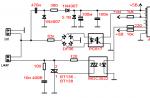
Memory circuit No. 6 (UC3843)

In diagram 6, a version of the PHI controller is made on the UC3843 (U1) chip, CA3130 op-amp (IC1), and LTV817 optocoupler. The current regulation in this version of the charger is carried out using a variable resistor PR1 at the input of the current amplifier of the U1 microcircuit, the output voltage is regulated using PR2 at the inverting input IC1.
There is a “reverse” reference voltage at the “direct” input of the op-amp. That is, regulation is carried out relative to the “+” power supply.
In schemes 5 and 6, the same sets of components (including chokes) were used in the experiments. According to the test results, all of the listed circuits are not much inferior to each other in the declared range of parameters (frequency/current/voltage). Therefore, a circuit with fewer components is preferable for repetition.
Memory circuit No. 7 (TL494)

The memory in diagram 7 was conceived as a bench device with maximum functionality, therefore there were no restrictions on the volume of the circuit and the number of adjustments. This version of the charger is also made on the basis of a PHI current and voltage regulator, like the option in diagram 4.
Additional modes have been introduced into the scheme.
1. “Calibration - charge” - for pre-setting the end voltage thresholds and repeating charging from an additional analog regulator.
2. “Reset” - to reset the charger to charge mode.
3. “Current - buffer” - to switch the regulator to current or buffer (limiting the output voltage of the regulator in the joint supply of the device with battery voltage and the regulator) charge mode.
A relay is used to switch the battery from the “charge” mode to the “load” mode.
Working with the memory is similar to working with previous devices. Calibration is carried out by switching the toggle switch to the “calibration” mode. In this case, the contact of the toggle switch S1 connects the threshold device and a voltmeter to the output of the integral regulator IC2. Having set the required voltage for the upcoming charging of a specific battery at the output of IC2, using PR3 (smoothly rotating) the HL2 LED lights up and, accordingly, relay K1 operates. By reducing the voltage at the output of IC2, HL2 is suppressed. In both cases, control is carried out by a built-in voltmeter. After setting the PU response parameters, the toggle switch is switched to charge mode.
Scheme No. 8
The use of a calibration voltage source can be avoided by using the memory itself for calibration. In this case, you should decouple the TS output from the SHI controller, preventing it from turning off when the battery charge is complete, determined by the TS parameters. The battery will one way or another be disconnected from the charger by the contacts of relay K1. The changes for this case are shown in Figure 8.
In calibration mode, toggle switch S1 disconnects the relay from the positive power supply to prevent inappropriate operations. In this case, the indication of the operation of the TC works.
Toggle switch S2 performs (if necessary) forced activation of relay K1 (only when calibration mode is disabled). Contact K1.2 is necessary to change the polarity of the ammeter when switching the battery to the load.
Thus, a unipolar ammeter will also monitor the load current. If you have a bipolar device, this contact can be eliminated.
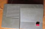
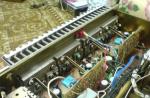
Charger design
In designs it is desirable to use as variable and tuning resistors multi-turn potentiometers to avoid suffering when setting the necessary parameters.
Design options are shown in the photo. The circuits were soldered impromptu onto perforated breadboards. All the filling is mounted in cases from laptop power supplies.
They were used in designs (they were also used as ammeters after minor modifications).
The cases are equipped with sockets for external connection of batteries, loads, and a jack for connecting an external power supply (from a laptop).

He designed several digital pulse duration meters, different in functionality and elemental base.
More than 30 improvement proposals for the modernization of units of various specialized equipment, incl. - power supply. For a long time now I have been increasingly involved in power automation and electronics.
Why am I here? Yes, because everyone here is the same as me. There is a lot of interest here for me, since I am not strong in audio technology, but I would like to have more experience in this area.
Reader vote

The article was approved by 77 readers.
To participate in the voting, register and log in to the site with your username and password.Quite relatively recently I decided to make a pair chargers for a car battery that I planned to sell on the local market. There were quite excellent industrial buildings available; you just had to make a good filling and that was it.
But then I encountered a sequence of troubles, starting from the power supply and ending with the output voltage control unit. I went and bought a good old electronic transformer like Tashibra (Chinese brand) for 105 watts and started remodeling.
Tashibra is an electronic (pulse) network power supply implemented on a half-bridge base, does not have any protection, and in addition there is no simple network filter. Upon completion of the alteration (more on this in the following articles), it was possible to obtain up to 18 Volts of direct voltage at the output of the transformer with a current of 8-10 Amps, which is more than enough to charge quite capacious car batteries.
The size of the board is no larger than a pack of cigarettes; the power supply ended up being quite compact and wonderful. The second trouble was related to the power regulator; it was impossible to charge the battery directly, so it was decided to use a simple PWM regulator circuit.
In the domestic circuit, the power link has a wonderful N-channel field-effect transistor, in my case IRFZ44, of course it is not critical, it is possible to use almost every similar switch with a permissible current of 20 Amperes or more.
Low-power transistors are also not critical, possible to apply each reverse conduction transistors (low power, such as KT3102, KT315, S9012/9014/9016/9018 and others), a multivibrator with an adjustable duty cycle of pulses is assembled on them, which controls a wonderful field switch.
The field-effect transistor will overheat during operation, but this overheating will not be too great, but just in case, the transistor should be installed on a heat sink.
This PWM output voltage regulator circuit can work perfectly with any chargers/ power supply, regardless of type, input voltage rating from 3.5 to high voltage allowed through a field-effect transistor (60-75 Volts, in some cases 100 and higher, it all depends on the specific transistor).
Required reading:
DIY PWM controller
Articles on exactly the topics you are interested in:
In previous articles, we looked at the design of a PWM power regulator, which is recommended for adjusting the output voltage of a charger or power supply. Now the appeal will be sent about...
Often, especially in winter, motorists are faced with the need to charge their car battery. Perhaps you need to buy a factory charger, it’s better...
PWM power regulator, an indispensable part of any power supply. The diagram below allows you to regulate the voltage of the power supply from 1 Volt to the limit voltage of the power supply (but...
Relatively not so long ago, I got a couple of computer power supplies for free, and to my surprise, some of them were completely working. It was decided to share the experience of redesigning the power supply...
At the moment, there are a large number of outdated system units with working power supplies. These blocks can be used for different purposes. This will require minor modifications. Me…